The first generation Intel processors used in PCs were 8-bit 8088 and 16-bit 8086 coming to the market around 1980. The 8088 dominated in sales since its 8-bit data bus required less costly motherboards than the 16-bit 8086 and most of the interface chips available at that time were intended for use in 8-bit designs. The 8086 was used in early IBM PS/2 models, but was never a popular choice for PCs. Both processors were capable of addressing 1MB of memory.
The second generation Intel processor was 16-bit 80286, used in IBM's AT system since 1982. The 286 provided significant performance increases over the 8088 and 8086 - double or more performance at the same clock speed. The 286 also widened the address bus to allow access to 16 MB of memory, and introduced protected mode operation. It was originally available in 6 MHz and 8 MHz versions, but was later expanded to faster versions, all the way up to 20 MHz.
The third generation processors are members of the 386 family available on the market from 1985 till early 1990's. The Intel 386DX was the first true 32-bit processor used on the PC platform. Its internal register size was increased to 32 bits, and its data and address buses were as well, doubling data path width to the processor and, in theory, increasing addressable memory to 4 GB. The 80386DX was also the first to use pipelining to allow much improved processor performance through the use of much higher clock frequencies (16 to 40MHz). Furthermore, the 386DX's increased power and the improved processor modes it offered (including full protected mode and virtual real modes) spurred the introduction of GUI-based operating systems on the PC, such as Microsoft Windows. However, the 386 did not offer the very large improvements over the 286 that the 286 did over the 8088.
The fourth generation is represented by the 486 family. The Intel 486DX chip had an integrated math coprocessor, which drastically boosted the speed of floating-point operations. In fact, the 486DX was the first chip suitable for math-intensive engineering and scientific computations, providing a very significant increase in power over the 386DX processor. The 486 processor was also the first to incorporate L1 cache on the chip, thus reducing the number of required accesses to memory. The 486 brought GUIs to the mainstream on PCs; it is the minimum processor that most people consider "usable" for running an operating system like Microsoft Windows. In later members of the 486 family, including DX2 and DX4, the "clock multiplying" technology started to be used, where the processor runs at a faster speed than the memory bus. The 486 processors were on the market from 1989 till 1994 and ran at clock speeds from 25 to 120MHz.
The fifth-generation chip was the Pentium. The Pentium had a number of the key architectural enhancements greatly increasing its performance over its predecessor, the 486 chip. Due to its superscalar architecture, with two parallel execution units in use, a Pentium chip was able to deliver double the speed of a 486 chip of the same clock speed. The Pentium's data bus also was doubled to 64 bits, providing double the bandwidth for transfers to and from memory. Moreover, most Pentiums ran on 60 or 66 MHz system buses, as compared to 25 to 40MHz buses in 486 systems. Pentiums also went to much higher clock speeds, up to 200 MHz. The floating point unit of the Pentium was redesigned and proved to be significantly faster than that of the 486. Pentiums were around from 1994 till 1997. The last member of the family was Pentium MMX (166 to 233MHz). The well-publicized difference between the Pentium MMX and the regular Pentium is the inclusion of the MMX instruction set extensions. Other improvements in the MMX design included doubled primary cache, improved cache mapping, deepening of internal pipelines, improved branch prediction unit, and improved instruction decoder. All these improvements resulted in approximately 20% performance boost over regular Pentium at the same clock speed.
The Pentium Pro introduced in 1995 as the successor to the Pentium can be classified as the six-generation chip. The Pentium Pro was the first mainstream CPU to radically change how it executes instructions, by translating them into RISC-like microinstructions and executing these on a highly advanced internal core. When running 32-bit applications, the Pentium Pro achieved performance approximately 50% higher than a Pentium of the same clock speed. In addition to its new way of processing instructions, the Pentium Pro incorporates several other technical advances, such as superpipelining, integrated L2 cache, 32-bit optimizations, wider address bus, giving it a maximum addressability of 64 GB of memory, greater multiprocessing, out-of-order completion, enhanced branch prediction unit, and speculative execution which greatly reduces pipeline stall time in its RISC core. The most widely-publicized advanced feature of the Pentium Pro is of course the integrated L2 cache. The majority of Pentium Pro's were manufactured in either 180 MHz or 200 MHz versions, the latter was available with 256 KB, 512 KB or 1 MB of L2 cache.
In 1997, Intel released the Pentium II, which was much an evolutionary step from the Pentium Pro. The Pentium II improves over the Pentium Pro architecturally in the following areas: higher clock speeds (233 to 300MHz), the addition of the MMX instruction set extensions, doubled L1 cache, segment register caches for improved 16-bit code execution, and deeper write buffers. In early 1998, Intel released the 333 MHz Pentium II, codenamed "Deschutes". This was the first Pentium II using the new 0.25 micron fabrication process, which dramatically reduces the die size and power consumption of the chip. Later, the bus speed was raised from 66 to 100MHz and new two new Pentium II processors running at clock speeds of 350 and 400 MHz introduced.
The Pentium III introduced in 1999 was in fact an enhanced version of Pentium II. The Pentium III on the Katmai core (Slot 1) was fitted with 512 KB external L2 cache and most common at 450 and 500MHz clock speeds. The Pentium III with Coppermine core (Socket 370) was available at speeds from 450 to 1333 MHz.
The latest member of the Pentium family, the Pentium IV, reflected the Intel's commitment to modernize the traditional x87 floating-point architecture. The Pentium IV benefited from a fully pipelined FPU stage allowing for floating-point instructions to be buffered and restructured before actual decode and execution initiates. The Pentium IV architecture made use of two floating-point execution units, leading to 25 to 50% performance gain over Pentium III. The Pentium IV also added support for the newly inducted SSE2 multimedia instruction set. Performance improvements and additional instructions make Pentium 4 Intel's most significant microprocessor enhancement since the introduction of Pentium II. Pentium IV processors at the clock speeds from 1300 to 3400 MHz and the bus speeds from 133 to 200MHz were manufactured from 2001 till 2004.
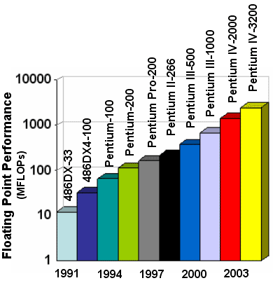
Floating-point performance of the Intel processors used in PCs has grown by two orders of magnitude over the past decade. Some results coming from a number of PCs I owned during this time are summarized the following figure:
The benchmark results presented are based on real-life engineering and quantum-chemical computations (carried out using the ODEPACK, MUDPACK, MOPAC, GAMESS and GAUSSIAN packages compiled using the Microsoft Fortran PowerStation 1.0 and 4.0 and the Compaq Visual Fortran 6.1). Such computations rely heavily on the floating point unit and the processor-memory bus. All numbers should be considered approximate, since system variations can cause a particular PC to score significantly above or below the benchmarks shown.